Digital Circuit Design
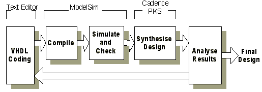
[Last modified 11:11:53 PM on Tuesday, 27 July 2010]An alternative, that is used is to describe the intended behaviour and architecture of a design, is by using a high level Hardware Description Language (HDL). The two competing standards, Verilog and VHDL, are HDLs which allow circuit designs to be represented in a way that is much more intuitive to create and understand. Furthermore, the designs can be created much more rapidly, and the only errors are likely to be with the logic design, as opposed to wrongly connected gates.
HDL designs can then be compiled into a vendor specific encoding, for use with simulation and testing tools. Once the design is believed to work correctly, a synthesis tool then processes it, to produce a design for an ASIC or FPGA chip. The resulting output is then analysed for performance data, the code may be refined and recompiled, and the process is repeated.
ASICs and FPGAs
Both Application Specific Integrated Circuits (ASICs) and Field Programmable Gate Arrays (FPGAs) are types of custom chips, which differ in their properties, cost, and in the way that they are manufactured. The choice of which to use depends on the required application.
FPGAs
FPGA devices typically contain an architecture that is vendor specific. A major advatage is that the designer is then able to quickly program them as required, with no additional manufacturing necessary. If testing fails, then the design can be changed and another device immediately reprogrammed. In addition, circuit design outside of the chip can be simultaneously performed since the function of FPGA pins can be assigned before the internal design is complete. However, FGPA devices cost on average between US$100 to US$200, making them relatively expensive for mass production.ASICs
Older style ASIC chips initially contained arrays of unconnected transistors, created during the most complex and costly phase of manufacture. Known as "gate arrays", these contained a set of basic cells across the chip, which included logic gates, registers, and macro functions such as multiplexors and comparators. Gate arrays may or may not contain predefined "channels", used for routing between the basic cells.The most common type of ASIC currently used is the standard cell format. These contain no components and the time of initial manufacture, and do not contain any type of basic cell. Instead, custom layouts are created for each part of the design, making more efficient use of the available silicon.
A final manufacturing process involves the connection of the generic units to form the specified design, and can take two or more weeks. Individual devices can cost as little as US$10, but the initial engineering costs can be US$20,000 to over US$100,000.
The designs described in this documents are targeted for ASIC chips, and make use of the TSMC 0.18mm Standard Cell Library.
References
- Douglas J. Smith, HDL Chip Design, Madison, AL, USA: Doone Publications, 1996, pp3-5